
Introduction to Vertical Surface Luminescent Chips in Laser Chips
Source: This website time:2021-08-27 browse:2258
Side emitting laser chips rely on the dissociation surface of the substrate crystal as the resonant cavity surface. The technology has matured for chips with high power and high energy requirements, but there are also many shortcomings, such as high requirements for the cavity surface in laser performance, which cannot be used for conventional wafer cutting, such as sanding wheel blades, laser cutting, etc.
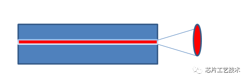
In actual production, the testing process is particularly complicated as it needs to be dissociated into bar bars in order to continue testing, which consumes the production capacity of slicing.
Therefore, many people want to develop laser chips that can emit lasers.
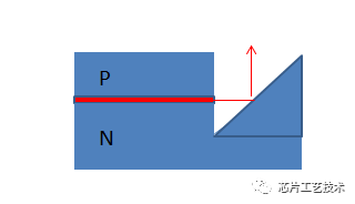
Etch the 45 ° mirror reflection side to emit light. The emission characteristics are completely dependent on the tilt angle and flatness of the internal reflector, which makes the manufacturing process difficult and has issues such as beam distortion. Many people have studied this in the early days, and Mems have also been used for mirror surface research, but it is difficult to mass produce.
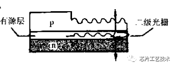
This is a high-order coupled grating SELD. Although it can obtain narrow and fine beams with small divergence angles, its emission interface has a strip-shaped structure. Due to the Bragg reflection effect, its longitudinal mode selectivity is good, which can achieve dynamic single longitudinal mode operation. However, most of the emitted light enters the substrate, greatly reducing efficiency, and the reflection angle of the laser beam varies with wavelength.
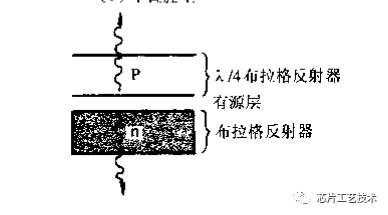
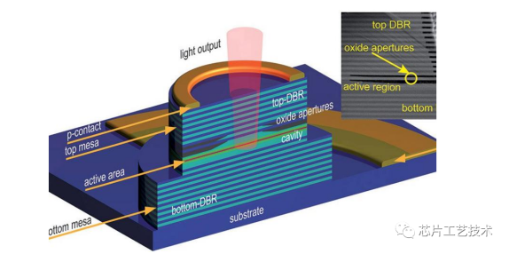
The third type is the Vcsel chip, which has an active area diameter and cavity length of only micrometers, making it easy to achieve low Ith and microampere current levels.
It has high differential quantum efficiency, small beam divergence angle, easy fiber coupling, and good dynamic single longitudinal mode and spatial emission mode performance.
The emission wavelength of Vcsel depends on epitaxial growth, rather than being completely determined by materials and chip processes, making it relatively easy to achieve accurate control of the emission wavelength. VCSEL arrays can be prepared and directly tested on the wafer surface.
The main difficulty in the development of high-power VCSEL lies in how to deal with thermal effects when the number of light-emitting holes increases. To optimize the epitaxial quantum well in the epitaxial direction, improve the internal quantum efficiency, optimize the thermal resistance of the epitaxial material, and improve the heat dissipation characteristics of the device; By optimizing the chip design structure in the chip direction, the photoelectric efficiency can be improved.
At present, the domestic Vcsel industry chain has become mature, and wafers can also achieve a scale of 6 inches. There are also signs of preparing for 8 inches. However, vcsel chips with long wavelengths such as 1310nm1550nm still face many problems because they require thicker DBR layers.
Copyright © 2019 安徽华创鸿度光电科技有限公司 版权所有 备案号:皖ICP备20001029号-1  皖公网安备 34010302002496号技术支持 科威鲸网络


